TODO: Add table of content
# MSLA PCB Exposure: KiCad → Photon Mono 4
## Why MSLA?
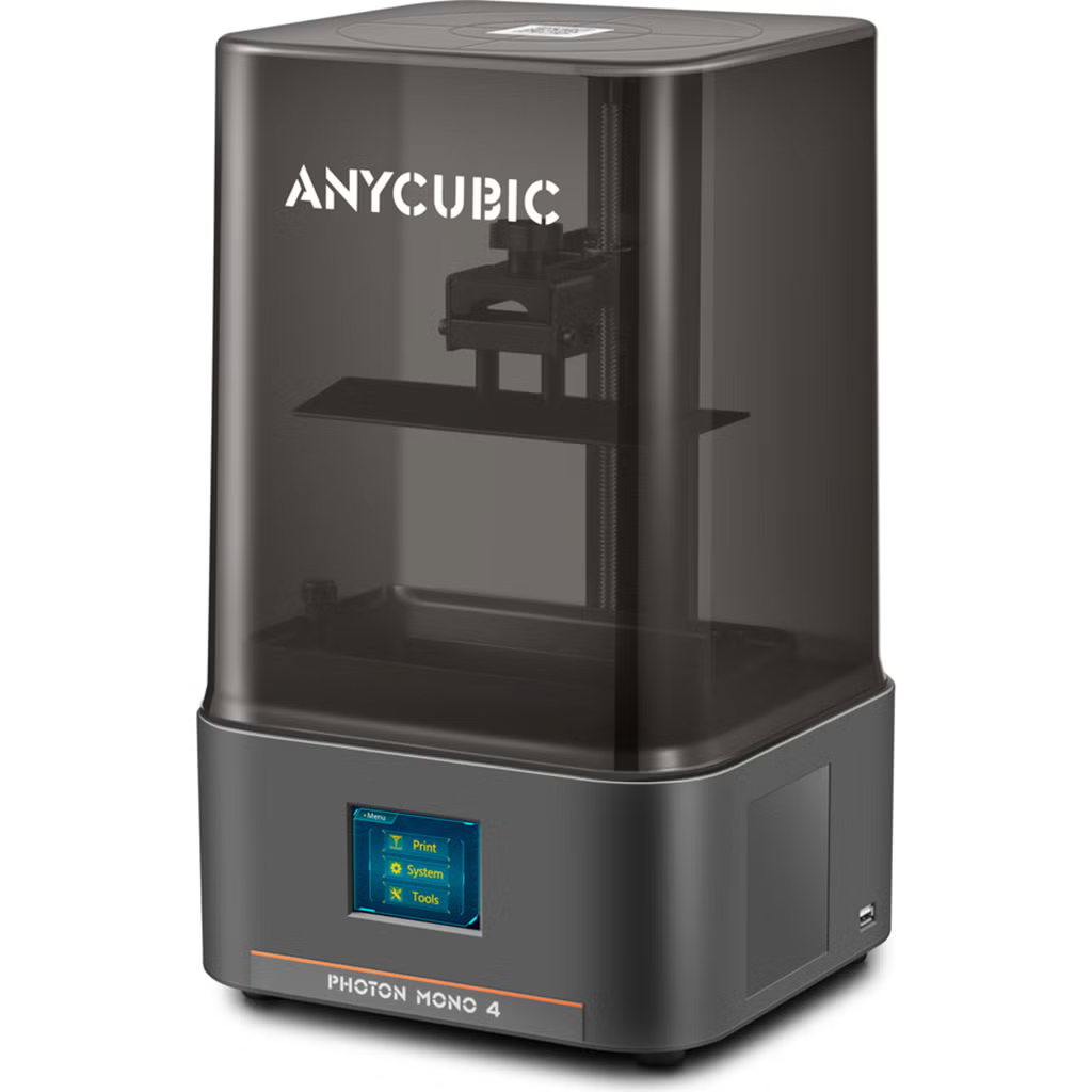
Using an MSLA (Masked Stereolithography Apparatus) resin printer for creating PCBs is a technique known as "Direct UV Exposure." Instead of printing a plastic part, you use the printer's LCD screen as a dynamic digital mask to cure photosensitive materials (etch resist, solder resist and silkscreen) on a copper board.
The "Matrix LED" ensures uniform light distribution across the entire build area. When exposing a photosensitized board, uneven lighting can cause some areas to be under-exposed (washing away traces) or over-exposed (causing traces to merge). The matrix source ensures the center and corners of your PCB receive the same energy, resulting in a reliable etch.
## The objective
KiCad PCB layers need to be converted to `.pm4n` files for direct UV exposure on an **Anycubic Photon Mono 4** (9024×5120 px, 17 µm/px, 1494.12 DPI) on the screen size of 153.408 x 87.040 mm.
## Hardware
* A resin 3D printer (e.g., Anycubic Photon Mono 4)
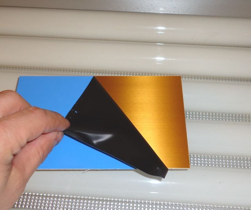
 * Photosensitive PCB. For consistent results, a pre-sensitized board like the **Bungard positive photoresist boards** is highly recommended due to its uniform coating. A good example is [Bungard 160x100 double-sided](https://www.conrad.sk/sk/p/bungard-120306z33-zakladny-material-dvojstranna-35-m-foto-vrstva-pozitiv-d-x-s-160-mm-x-100-mm-1-ks-529176.html) 3,49 €.
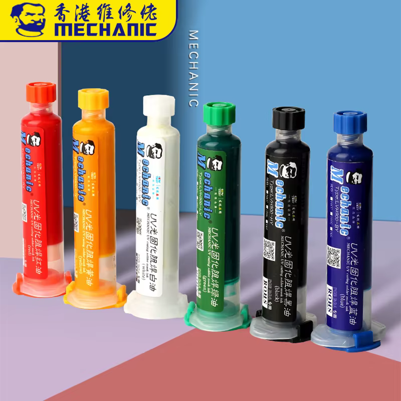
 * UV light curing Solder Mask e.g. from Mechanic. Use green as the solder mask and white for the silkscreen.
 ## Software
### 1. Install KiCad
Ensure you have kicad installed:
```bash
sudo apt update
sudo apt install kicad
```
### 2. KiCad: Set your design grid (Optional)
In KiCad's PCB editor, go to `Preferences → Preferences → PCB Editor → Grids` and add a custom grid of 0.017 mm (your MSLA printer's pixel size). This ensures trace edges land on pixel boundaries and avoids the sub-pixel rounding that causes the ±1px size error people see with arbitrary grids.
### 3. Export gerbers from KiCad
*If you want to automate the conversion of gerber to printing files, you can jump to the section [Appendix: Automated script](#appendix-automated-script).*
- Open your PCB project in the KiCad PCB Editor.
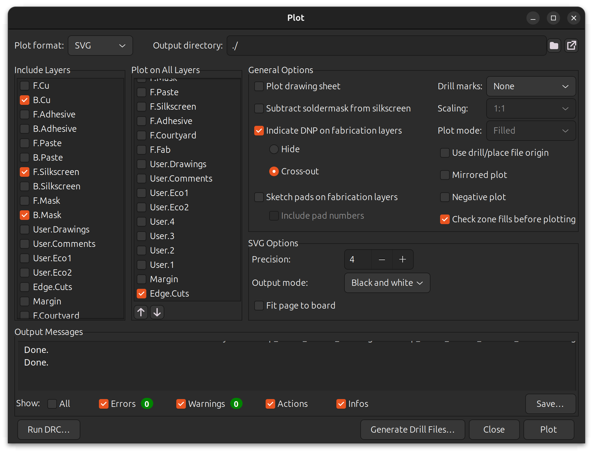
- Go to **File -> Plot** and select `Plot format` as `SVG` and set the `Output directory`.
- In the `Include Layers` section select layers `F.Cu`, `B.Cu`, `B.Mask` and `F.Silkscreen`. Each layer will be ploted as a separate SVG file.
- Optionaly, select additional layer(s) e.g. `Edge.Cuts` in the `Plot on All Layers` section. This way you can merge layers i.e. add board outset into each file generated. *This is usually not needed.*
- Click **Plot** and **Close**.
## Software
### 1. Install KiCad
Ensure you have kicad installed:
```bash
sudo apt update
sudo apt install kicad
```
### 2. KiCad: Set your design grid (Optional)
In KiCad's PCB editor, go to `Preferences → Preferences → PCB Editor → Grids` and add a custom grid of 0.017 mm (your MSLA printer's pixel size). This ensures trace edges land on pixel boundaries and avoids the sub-pixel rounding that causes the ±1px size error people see with arbitrary grids.
### 3. Export gerbers from KiCad
*If you want to automate the conversion of gerber to printing files, you can jump to the section [Appendix: Automated script](#appendix-automated-script).*
- Open your PCB project in the KiCad PCB Editor.
- Go to **File -> Plot** and select `Plot format` as `SVG` and set the `Output directory`.
- In the `Include Layers` section select layers `F.Cu`, `B.Cu`, `B.Mask` and `F.Silkscreen`. Each layer will be ploted as a separate SVG file.
- Optionaly, select additional layer(s) e.g. `Edge.Cuts` in the `Plot on All Layers` section. This way you can merge layers i.e. add board outset into each file generated. *This is usually not needed.*
- Click **Plot** and **Close**.
 ### 4. Install `CHITUBOX Basic`
Follow the [offical installatin guide for Ubuntu](https://docs.chitubox.com/en-US/chitubox-basic/latest/installation#ubuntu)
### 5. Create the `Dummy.pm4n` file
Open `CHITUBOX Basic` slicer (or any other slicer that works for your resin printer), select printer **Anycubic Photon Mono 4**, slice any tiny STL (e.g.: 1×1×0.05 mm box), and save as `Dummy.pm4n`.
This file is reused for every job — it carries the correct LCD resolution metadata.
## MSLA PCB Exposure
`UVtools` has a dedicated `PCB Exposure` tool that converts a Gerber file to a pixel-perfect image given your printer's LCD resolution, specifically for exposing copper traces.
### 1. Install `UVtools`
```bash
sudo apt-get install -y curl
sudo bash -c "$(curl -fsSL https://raw.githubusercontent.com/sn4k3/UVtools/master/Scripts/install-dependencies.sh)"
```
### 2. Run `UVtools`
```bash
cd UVtools
./UVtools
```
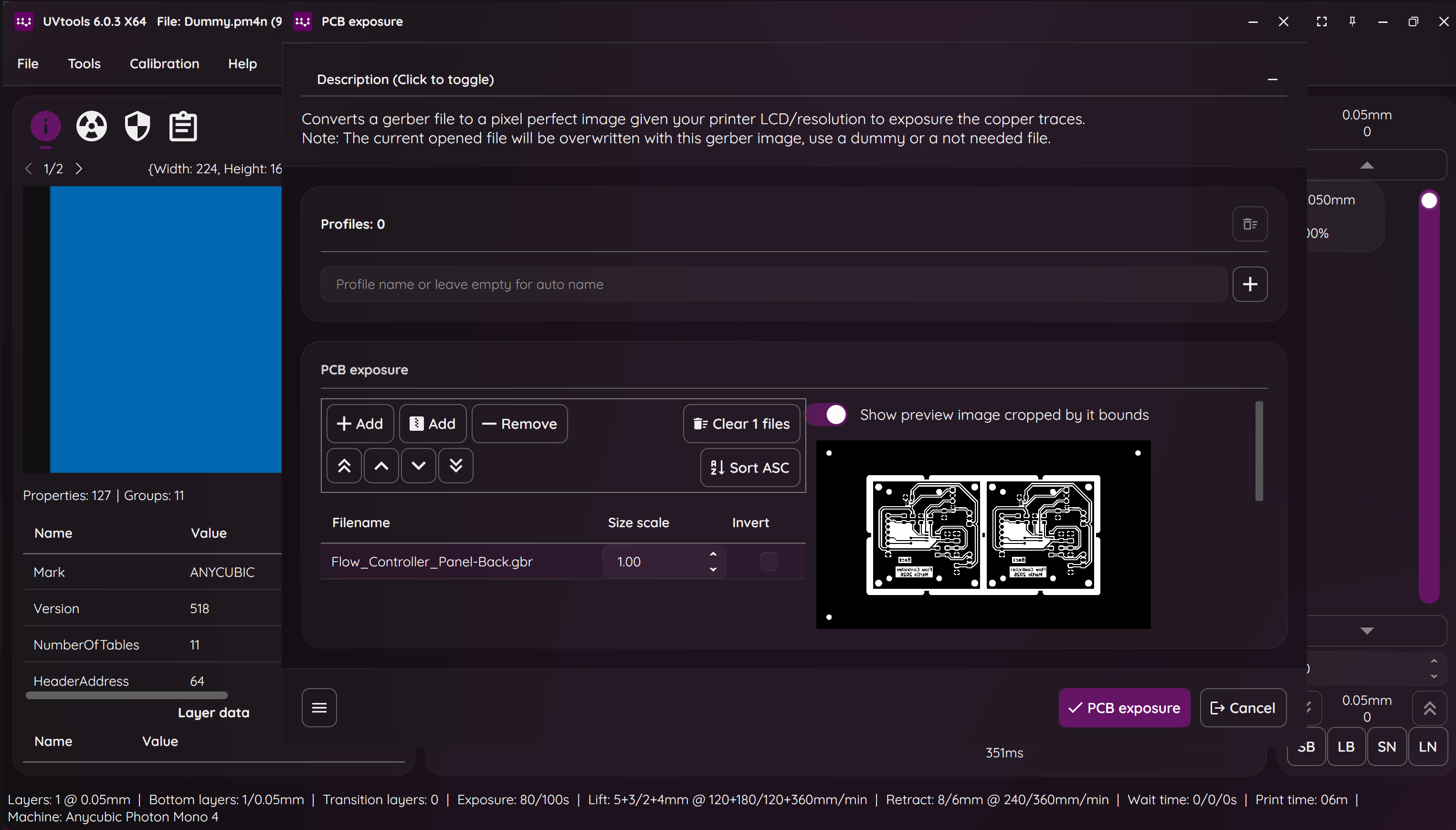
### 3. Export `.pm4n` file from Gerber layer
- You export Gerber from KiCad (not SVG), which natively gives you positive/negative control per layer.
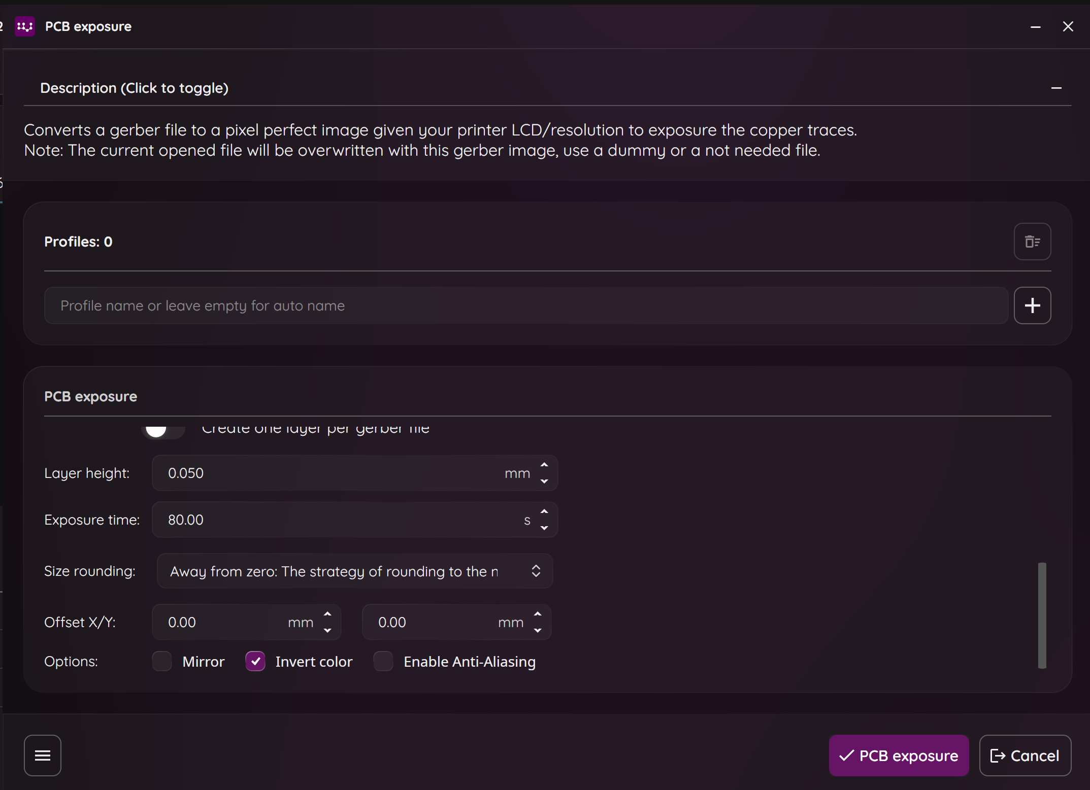
- You open the `Dummy.pm4n` file in `UVtools` (a minimal valid `.pm4n` sliced by `Chitubox` or `Photon Workshop` with any tiny model), then use `Tools → PCB Exposure` to inject your Gerber layer e.g.: `Flow_Controller_Panel-Front.gbr`.
- You control `inversion`, `invert` and the `exposure time` at the bottom of the `PCB exposure` dialog.
- You save it as e.g.: `Flow_Controller_Panel-Front.pm4n` file.
### 4. Install `CHITUBOX Basic`
Follow the [offical installatin guide for Ubuntu](https://docs.chitubox.com/en-US/chitubox-basic/latest/installation#ubuntu)
### 5. Create the `Dummy.pm4n` file
Open `CHITUBOX Basic` slicer (or any other slicer that works for your resin printer), select printer **Anycubic Photon Mono 4**, slice any tiny STL (e.g.: 1×1×0.05 mm box), and save as `Dummy.pm4n`.
This file is reused for every job — it carries the correct LCD resolution metadata.
## MSLA PCB Exposure
`UVtools` has a dedicated `PCB Exposure` tool that converts a Gerber file to a pixel-perfect image given your printer's LCD resolution, specifically for exposing copper traces.
### 1. Install `UVtools`
```bash
sudo apt-get install -y curl
sudo bash -c "$(curl -fsSL https://raw.githubusercontent.com/sn4k3/UVtools/master/Scripts/install-dependencies.sh)"
```
### 2. Run `UVtools`
```bash
cd UVtools
./UVtools
```
### 3. Export `.pm4n` file from Gerber layer
- You export Gerber from KiCad (not SVG), which natively gives you positive/negative control per layer.
- You open the `Dummy.pm4n` file in `UVtools` (a minimal valid `.pm4n` sliced by `Chitubox` or `Photon Workshop` with any tiny model), then use `Tools → PCB Exposure` to inject your Gerber layer e.g.: `Flow_Controller_Panel-Front.gbr`.
- You control `inversion`, `invert` and the `exposure time` at the bottom of the `PCB exposure` dialog.
- You save it as e.g.: `Flow_Controller_Panel-Front.pm4n` file.

 ### 4. Check the printer exposure
Open Chitubox
```Bash
cd /opt/CBD/CHITUBOX_Basic
./CHITUBOX_Basic.sh
```
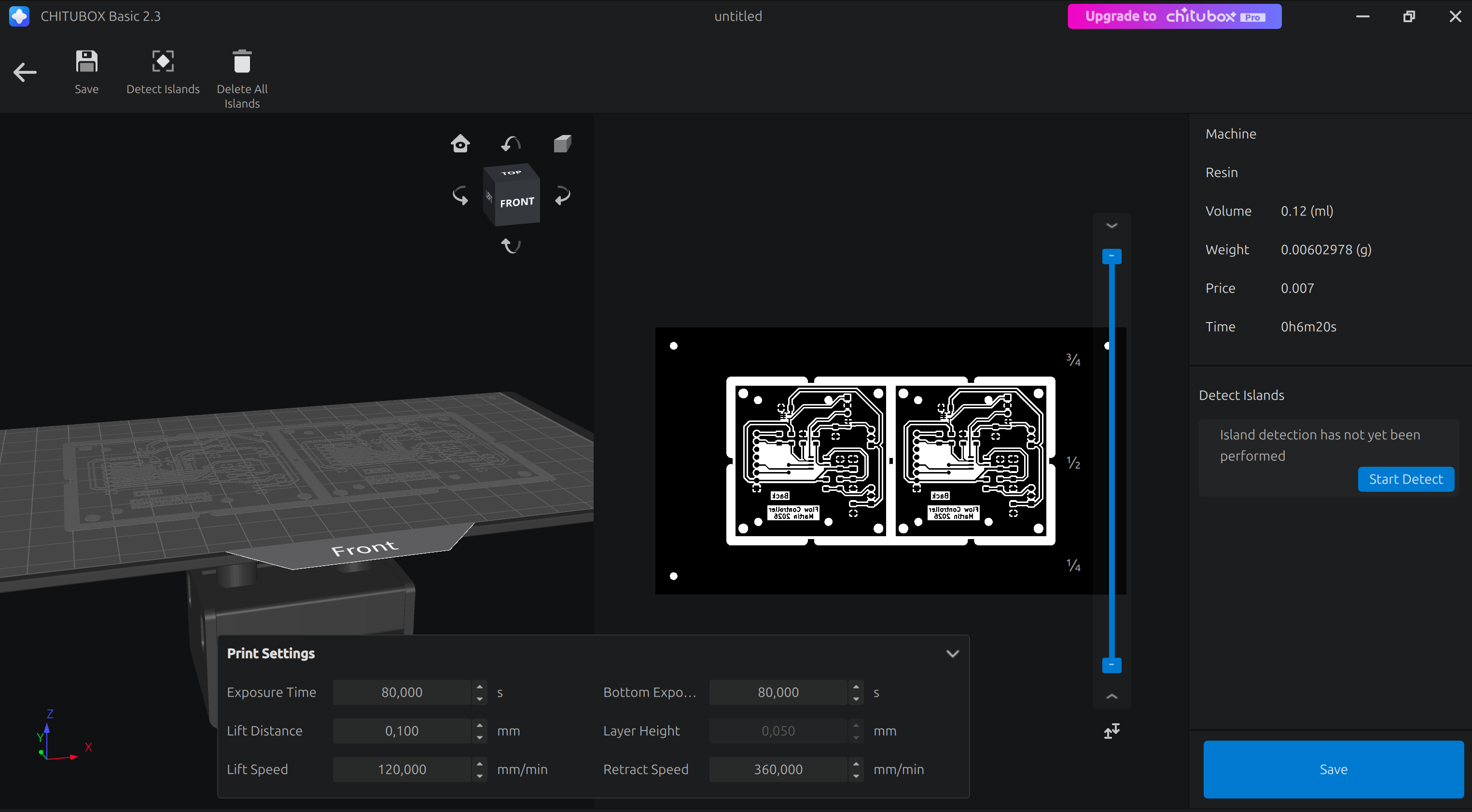
Open the `Flow_Controller_Panel-Front.pm4n` file to visually verify before printing.
### 4. Check the printer exposure
Open Chitubox
```Bash
cd /opt/CBD/CHITUBOX_Basic
./CHITUBOX_Basic.sh
```
Open the `Flow_Controller_Panel-Front.pm4n` file to visually verify before printing.
 *If you want to automate the conversion of gerber to printing files, you can jump to the section [Appendix: Automated script](#appendix-automated-script).*
### 5. Print
Place the presensitized copper board on the **Anycubic Photon Mono 4** printer's LCD screen. Copy the file `Flow_Controller_Panel-Front.pm4n` on the USB drive and 3D print it.
### 6. Developing
1. After exposure, you must develop the board to reveal the pattern.
* For a **positive photoresist board** (like the Bungard brand), the developer is a weak alkaline solution. A common and effective developer is a **1% solution of Sodium Hydroxide (NaOH)** in distilled or demineralised water.
* For the **UV light curing solder mask**, allow more time to it to harden. Clean the uncured part with Izopropanol afterwards.
2. **Safety First:** When working with chemicals like NaOH, always wear gloves and eye protection.
3. Submerge the board in the developer solution and gently agitate it. This should take 30-90 seconds, depending on the resist and developer freshness.
4. Rinse the board thoroughly with water.
### 7. Etching
For the developed Bungard photoresist PCB, etch the board using either `sodium persulfate` or `ferric chloride`.
- For `sodium persulfate`, prepare a solution with approximately 200–250 g/L and heat it to 40–50 °C.
- For `ferric chloride`, use a ready-to-use solution or prepare it according to the manufacturer's instructions and maintain a temperature of 35–45 °C.
Immerse the board in the etchant and agitate gently until all exposed copper has been removed, typically within 5–15 minutes. Rinse the board thoroughly with water after etching. To remove the remaining photoresist, immerse the board in a 2–5% `sodium hydroxide (NaOH)` solution at room temperature for 1–2 minutes, then rinse thoroughly with water and dry the board.
### 8. Drilling holes and milling board outlines
Use the project [kicad2gcode](https://gitea.virtonline.eu/2HoursProject/kicad2gcode) to generate G-Code for CNC driling and outlines milling.
---
## Appendix: Automated script
Automate the conversion from KiCAD to print files using a CLI.
### 1. The `Dummy.pm4n` file
Make sure you have the `Dummy.pm4n` file specific to your printer. See the section [5. Create the `Dummy.pm4n` file](#5-create-the-dummypm4n-file) above.
### 2. Install UVtools wrapper
Follow the UVtools wrapper [installation guide](UVtools/Readme.md)
### 3. Export KiCAD gerbers
```bash
kicad-cli pcb export gerbers \
-o gerbers \
-l F.Cu,B.Cu,F.Mask,B.Mask,F.SilkS,B.SilkS \
../kicad2panel/panel/Flow_Controller_Panel.kicad_pcb
```
Output:
```bash
Plotted to 'gerbers/Flow_Controller_Panel-Front.gtl'.
Plotted to 'gerbers/Flow_Controller_Panel-Back.gbl'.
Plotted to 'gerbers/Flow_Controller_Panel-F_Silkscreen.gto'.
Plotted to 'gerbers/Flow_Controller_Panel-B_Silkscreen.gbo'.
Plotted to 'gerbers/Flow_Controller_Panel-F_Mask.gts'.
Plotted to 'gerbers/Flow_Controller_Panel-B_Mask.gbs'.
```
### 4. Exposure
We need to **invert all** layers: `F.Cu,B.Cu,F.Mask,B.Mask,F.SilkS,B.SilkS`.
We need to **mirror all front** layers: `F.Cu,F.Mask,F.SilkS`.
Traces should appear black on white background.
- background = UV exposed = resist removed = etched away
- traces = dark = resist kept = copper stays
Start with `--exposure 60` and bracket from there — Bungard presensitized at 405nm typically lands between 30–120s depending on board vintage and storage.
Export the front and back **copper** layers for 120 seconds exposure
```bash
pcb-expose.sh Dummy.pm4n gerbers/Flow_Controller_Panel-Front.gtl \
--invert --mirror --exposure 120 \
--output pm4n/Flow_Controller_Panel-Front.pm4n
pcb-expose.sh Dummy.pm4n gerbers/Flow_Controller_Panel-Back.gtl \
--invert --exposure 120 \
--output pm4n/Flow_Controller_Panel-Back.pm4n
```
Export the front and back **soldermask** layers for 300 seconds exposure
```bash
pcb-expose.sh Dummy.pm4n gerbers/Flow_Controller_Panel-F_Mask.gtl \
--invert --mirror --exposure 300 \
--output pm4n/Flow_Controller_Panel-F_Mask.pm4n
pcb-expose.sh Dummy.pm4n gerbers/Flow_Controller_Panel-B_Mask.gtl \
--invert --exposure 300 \
--output pm4n/Flow_Controller_Panel-B_Mask.pm4n
```
Export the front and back **silkscreen** layers for 300 seconds exposure
```bash
pcb-expose.sh Dummy.pm4n gerbers/Flow_Controller_Panel-F_Silkscreen.gtl \
--invert --mirror --exposure 300 \
--output pm4n/Flow_Controller_Panel-F_Silkscreen.pm4n
pcb-expose.sh Dummy.pm4n gerbers/Flow_Controller_Panel-B_Silkscreen.gtl \
--invert --exposure 300 \
--output pm4n/Flow_Controller_Panel-B_Silkscreen.pm4n
```
### 5. Verify
Open the `.pm4n` files in **Chitubox Basic** slicer to visually verify before printing. See the section [4. Check the printer exposure](#4-check-the-printer-exposure).
---
## Troubleshooting
**`kicad-cli: command not found`** — add KiCad to PATH:
```bash
export PATH="/usr/lib/kicad/bin:$PATH"
```
Or on Flatpak:
```bash
alias kicad-cli='flatpak run --command=kicad-cli org.kicad.KiCad'
```
**Expected Gerber not found** — KiCad's layer→filename mapping:
| Layer | Filename stem |
|---|---|
| `F.Cu` | `Front` |
| `B.Cu` | `Back` |
| `F.Mask` | `F_Mask` |
| `B.Mask` | `B_Mask` |
| `F.SilkS` | `F_Silkscreen` |
---
*If you want to automate the conversion of gerber to printing files, you can jump to the section [Appendix: Automated script](#appendix-automated-script).*
### 5. Print
Place the presensitized copper board on the **Anycubic Photon Mono 4** printer's LCD screen. Copy the file `Flow_Controller_Panel-Front.pm4n` on the USB drive and 3D print it.
### 6. Developing
1. After exposure, you must develop the board to reveal the pattern.
* For a **positive photoresist board** (like the Bungard brand), the developer is a weak alkaline solution. A common and effective developer is a **1% solution of Sodium Hydroxide (NaOH)** in distilled or demineralised water.
* For the **UV light curing solder mask**, allow more time to it to harden. Clean the uncured part with Izopropanol afterwards.
2. **Safety First:** When working with chemicals like NaOH, always wear gloves and eye protection.
3. Submerge the board in the developer solution and gently agitate it. This should take 30-90 seconds, depending on the resist and developer freshness.
4. Rinse the board thoroughly with water.
### 7. Etching
For the developed Bungard photoresist PCB, etch the board using either `sodium persulfate` or `ferric chloride`.
- For `sodium persulfate`, prepare a solution with approximately 200–250 g/L and heat it to 40–50 °C.
- For `ferric chloride`, use a ready-to-use solution or prepare it according to the manufacturer's instructions and maintain a temperature of 35–45 °C.
Immerse the board in the etchant and agitate gently until all exposed copper has been removed, typically within 5–15 minutes. Rinse the board thoroughly with water after etching. To remove the remaining photoresist, immerse the board in a 2–5% `sodium hydroxide (NaOH)` solution at room temperature for 1–2 minutes, then rinse thoroughly with water and dry the board.
### 8. Drilling holes and milling board outlines
Use the project [kicad2gcode](https://gitea.virtonline.eu/2HoursProject/kicad2gcode) to generate G-Code for CNC driling and outlines milling.
---
## Appendix: Automated script
Automate the conversion from KiCAD to print files using a CLI.
### 1. The `Dummy.pm4n` file
Make sure you have the `Dummy.pm4n` file specific to your printer. See the section [5. Create the `Dummy.pm4n` file](#5-create-the-dummypm4n-file) above.
### 2. Install UVtools wrapper
Follow the UVtools wrapper [installation guide](UVtools/Readme.md)
### 3. Export KiCAD gerbers
```bash
kicad-cli pcb export gerbers \
-o gerbers \
-l F.Cu,B.Cu,F.Mask,B.Mask,F.SilkS,B.SilkS \
../kicad2panel/panel/Flow_Controller_Panel.kicad_pcb
```
Output:
```bash
Plotted to 'gerbers/Flow_Controller_Panel-Front.gtl'.
Plotted to 'gerbers/Flow_Controller_Panel-Back.gbl'.
Plotted to 'gerbers/Flow_Controller_Panel-F_Silkscreen.gto'.
Plotted to 'gerbers/Flow_Controller_Panel-B_Silkscreen.gbo'.
Plotted to 'gerbers/Flow_Controller_Panel-F_Mask.gts'.
Plotted to 'gerbers/Flow_Controller_Panel-B_Mask.gbs'.
```
### 4. Exposure
We need to **invert all** layers: `F.Cu,B.Cu,F.Mask,B.Mask,F.SilkS,B.SilkS`.
We need to **mirror all front** layers: `F.Cu,F.Mask,F.SilkS`.
Traces should appear black on white background.
- background = UV exposed = resist removed = etched away
- traces = dark = resist kept = copper stays
Start with `--exposure 60` and bracket from there — Bungard presensitized at 405nm typically lands between 30–120s depending on board vintage and storage.
Export the front and back **copper** layers for 120 seconds exposure
```bash
pcb-expose.sh Dummy.pm4n gerbers/Flow_Controller_Panel-Front.gtl \
--invert --mirror --exposure 120 \
--output pm4n/Flow_Controller_Panel-Front.pm4n
pcb-expose.sh Dummy.pm4n gerbers/Flow_Controller_Panel-Back.gtl \
--invert --exposure 120 \
--output pm4n/Flow_Controller_Panel-Back.pm4n
```
Export the front and back **soldermask** layers for 300 seconds exposure
```bash
pcb-expose.sh Dummy.pm4n gerbers/Flow_Controller_Panel-F_Mask.gtl \
--invert --mirror --exposure 300 \
--output pm4n/Flow_Controller_Panel-F_Mask.pm4n
pcb-expose.sh Dummy.pm4n gerbers/Flow_Controller_Panel-B_Mask.gtl \
--invert --exposure 300 \
--output pm4n/Flow_Controller_Panel-B_Mask.pm4n
```
Export the front and back **silkscreen** layers for 300 seconds exposure
```bash
pcb-expose.sh Dummy.pm4n gerbers/Flow_Controller_Panel-F_Silkscreen.gtl \
--invert --mirror --exposure 300 \
--output pm4n/Flow_Controller_Panel-F_Silkscreen.pm4n
pcb-expose.sh Dummy.pm4n gerbers/Flow_Controller_Panel-B_Silkscreen.gtl \
--invert --exposure 300 \
--output pm4n/Flow_Controller_Panel-B_Silkscreen.pm4n
```
### 5. Verify
Open the `.pm4n` files in **Chitubox Basic** slicer to visually verify before printing. See the section [4. Check the printer exposure](#4-check-the-printer-exposure).
---
## Troubleshooting
**`kicad-cli: command not found`** — add KiCad to PATH:
```bash
export PATH="/usr/lib/kicad/bin:$PATH"
```
Or on Flatpak:
```bash
alias kicad-cli='flatpak run --command=kicad-cli org.kicad.KiCad'
```
**Expected Gerber not found** — KiCad's layer→filename mapping:
| Layer | Filename stem |
|---|---|
| `F.Cu` | `Front` |
| `B.Cu` | `Back` |
| `F.Mask` | `F_Mask` |
| `B.Mask` | `B_Mask` |
| `F.SilkS` | `F_Silkscreen` |
---