# Content
- [Using a Resin 3D Printer for PCB Exposure](#using-a-resin-3d-printer-for-pcb-exposure)
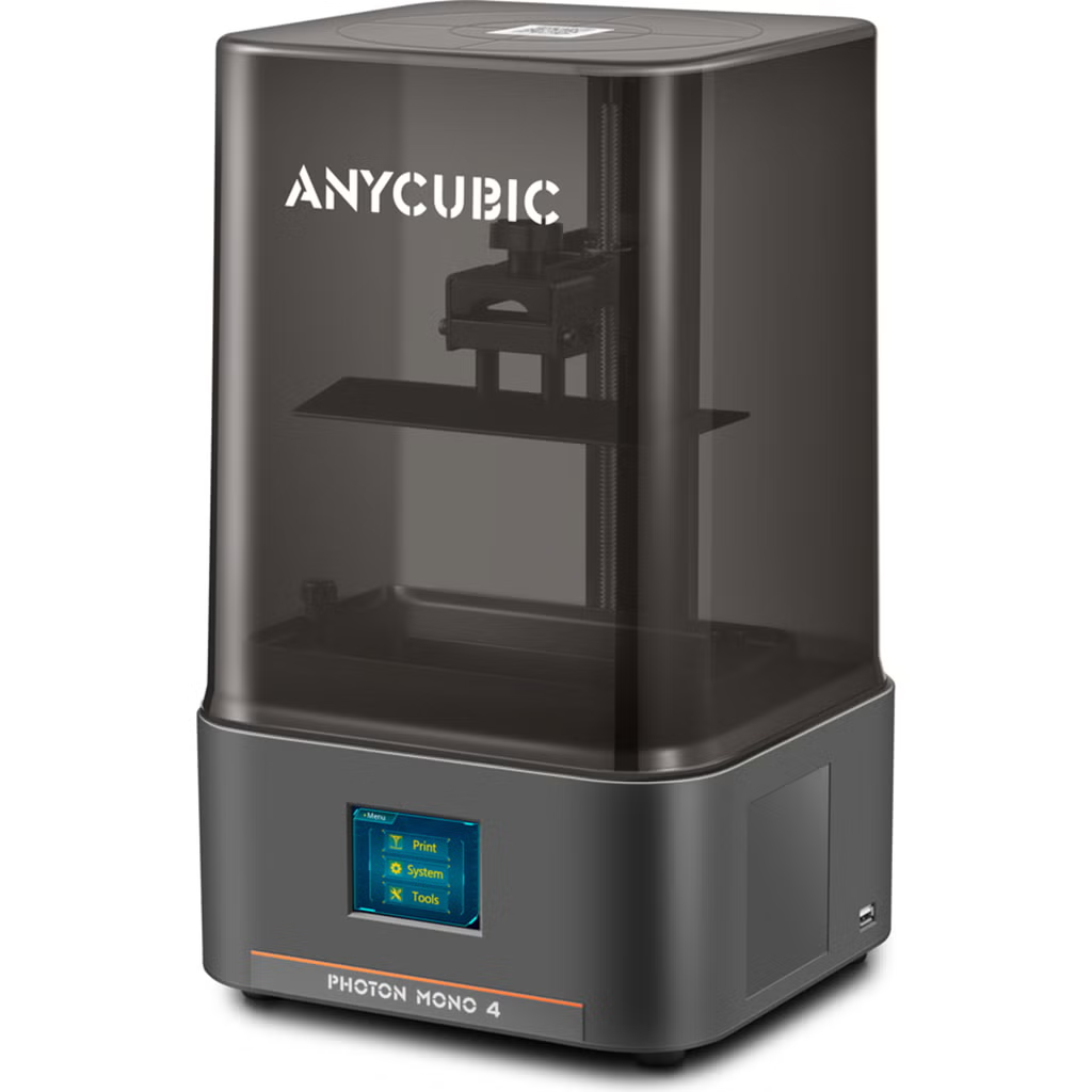
- [The Printer: Anycubic Photon Mono 4](#the-printer-anycubic-photon-mono-4)
- [Technical Specifications](#technical-specifications)
- [Why is it a good tool for DIY PCBs?](#why-is-it-a-good-tool-for-diy-pcbs)
- [Workflow Overview](#workflow-overview)
- [Prerequisites](#prerequisites)
- [Software](#software)
- [Hardware](#hardware)
- [Step-by-Step Guide](#step-by-step-guide)
- [Installation](#installation)
- [1. Export Layers from KiCad](#1-export-layers-from-kicad)
- [2. SVG to STL Conversion](#2-svg-to-stl-conversion)
- [Manual Conversion](#manual-conversion)
- [Automated Conversion](#automated-conversion)
- [3. Slicing in Chitubox](#3-slicing-in-chitubox)
- [4. Exposing the Board](#4-exposing-the-board)
- [5. Developing](#5-developing)
# Using a Resin 3D Printer for PCB Exposure
This guide documents the process of using a resin 3D printer, such as the Anycubic Photon Mono 4, as a UV light source to expose photosensitive materials like pre-sensitized copper boards or solder masks. The printer's LCD screen acts as a precise digital mask.
## The Printer: Anycubic Photon Mono 4
Based on the user manual, here are the technical specifications for the printer, followed by an analysis of why this specific machine is excellent for DIY PCB fabrication.
### Technical Specifications
* **System:** Photon Mono 4
* **Screen / Display:** 7-inch 10K Monochrome LCD
* **Resolution (XY):** 9024 x 5120 pixels
* **Light Source:** Matrix LED light source (405nm wavelength)
* **Build Volume:** 153.4 mm (L) x 87 mm (W) x 165 mm (H)
* **Z-Axis Accuracy:** 0.01 mm
* **Layer Thickness:** 0.01 ~ 0.15 mm
* **Connectivity:** USB Type-A (2.0)
* **Machine Dimensions:** 230 mm x 235 mm x 391 mm
* **Weight:** 4 kg
### Why is it a good tool for DIY PCBs?
Using an MSLA (Masked Stereolithography) resin printer for creating PCBs is a technique known as "Direct UV Exposure." Instead of printing a plastic part, you use the printer's LCD screen as a dynamic digital mask to cure photosensitive materials on a copper board.
Here is why the **Anycubic Photon Mono 4** specifically is well-suited for this task:
**1. Extremely High Resolution (10K Screen)**
The standout feature of this printer is the **10K (9024 x 5120)** resolution with a pixel size of 17µm (0.017mm) on a 7-inch screen.
* **Why it helps:** In PCB fabrication, resolution dictates how thin your traces can be. A 10K screen provides an exceptionally small pixel pitch. To put this in perspective, this is equivalent to a print resolution of approximately **1500 DPI**.
* *Calculation: The screen width is 153.4mm (6.04 inches). 9024 pixels / 6.04 inches ≈ 1494 DPI.*
* This allows you to expose traces for fine-pitch SMD components (like TQFP or 0402 packages) with professional-grade sharpness, far exceeding what is possible with inkjet or laser-printed transparencies.
**2. Uniform Light Source**
* **Why it helps:** The "Matrix LED" ensures uniform light distribution across the entire build area. When exposing a photosensitized board, uneven lighting can cause some areas to be under-exposed (washing away traces) or over-exposed (causing traces to merge). The matrix source ensures the center and corners of your PCB receive the same energy, resulting in a reliable etch.
**3. Perfect Wavelength (405nm)**
* **Why it helps:** The UV LEDs in resin printers operate at **405nm**. This wavelength is perfectly compatible with most standard dry film photoresists and UV-curable solder masks used in PCB manufacturing. You do not need to modify the light source.
## Workflow Overview
The process involves exporting 2D layer images from your PCB design, converting them into a flat 3D model, and then "printing" this model with specific exposure settings in your slicer.
## Prerequisites
### Software
* KiCad (for PCB design and SVG export)
* Inkscape (for SVG manipulation)
* Blender (for 3D model creation)
* Chitubox (or your printer's slicing software)
### Hardware
* A resin 3D printer (e.g., Anycubic Photon Mono 4)
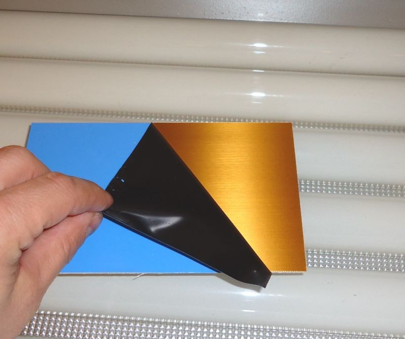
 * Photosensitive PCB. For consistent results, a pre-sensitized board like the **Bungard positive photoresist boards** is highly recommended due to its uniform coating. A good example is [Bungard 16x100 double sided](https://www.conrad.sk/sk/p/bungard-120306z33-zakladny-material-dvojstranna-35-m-foto-vrstva-pozitiv-d-x-s-160-mm-x-100-mm-1-ks-529176.html).
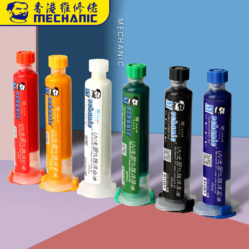
 * UV light curing Solder Mask e.g. from Mechanic. Use green as the solder mask and white for the silkscreen.
 ### Installation
Ensure you have both installed:
```bash
sudo apt update
sudo apt install inkscape blender
```
Make sure you have recent versions installed:
```bash
inkscape --version
blender --version
```
This guide was developed to work with Inkscape 1.2.2 and Blender 5.0.0
## Step-by-Step Guide
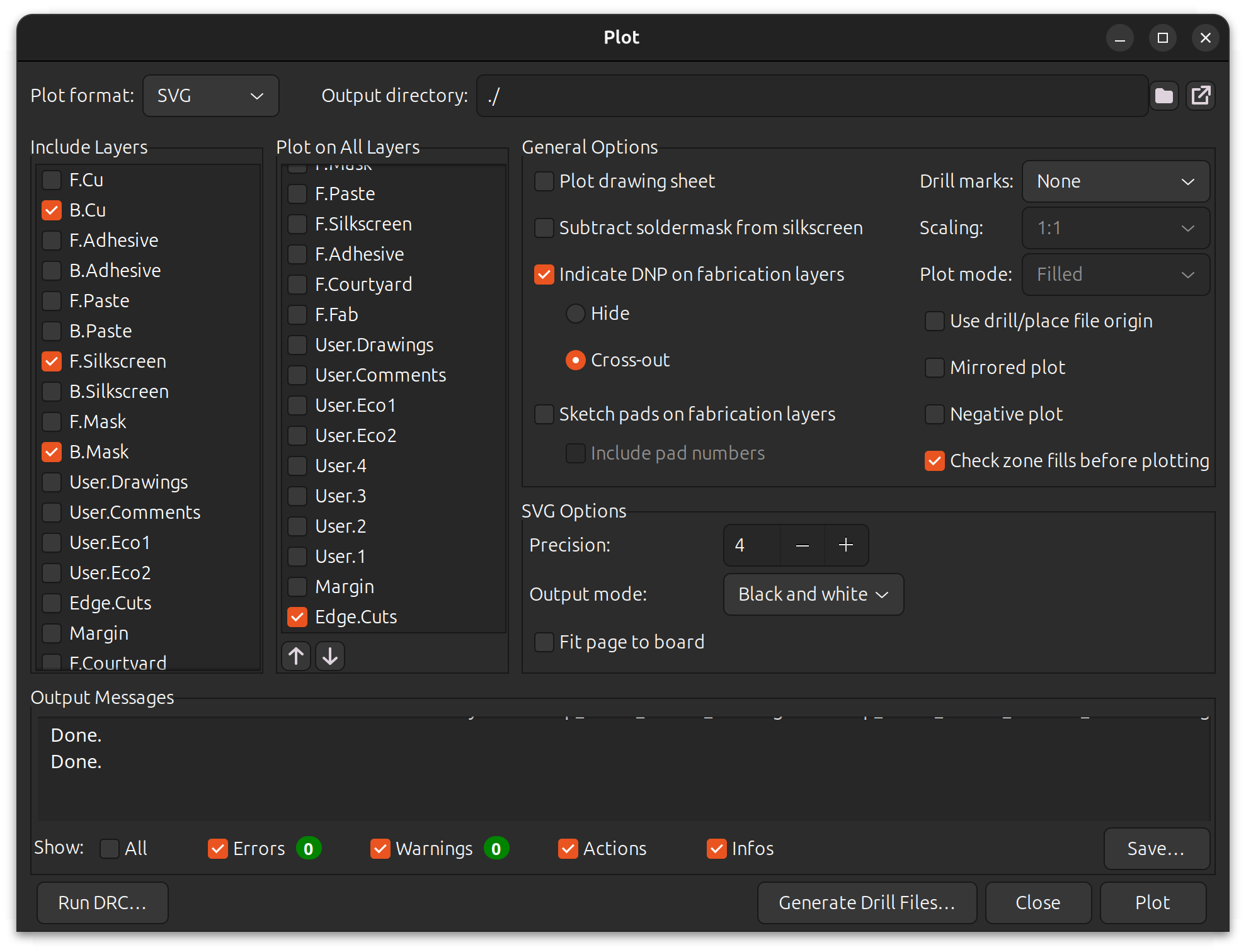
### 1. Export Layers from KiCad
1. Open your PCB project in the KiCad PCB Editor.
2. Go to **File -> Plot** and select `Plot format` as `SVG` and set the `Output directory`.
3. In the `Include Layers` section select layers `B.Cu`, `B.Mask` and `F.Silkscreen`. Each layer will be ploted as a separate SVG file.
4. Optionaly, select additional layer(s) e.g. `Edge.Cuts` in the `Plot on All Layers` section. This way you can merge layers i.e. add board outset into each file generated.
5. Click **Plot** and **Close**.
### Installation
Ensure you have both installed:
```bash
sudo apt update
sudo apt install inkscape blender
```
Make sure you have recent versions installed:
```bash
inkscape --version
blender --version
```
This guide was developed to work with Inkscape 1.2.2 and Blender 5.0.0
## Step-by-Step Guide
### 1. Export Layers from KiCad
1. Open your PCB project in the KiCad PCB Editor.
2. Go to **File -> Plot** and select `Plot format` as `SVG` and set the `Output directory`.
3. In the `Include Layers` section select layers `B.Cu`, `B.Mask` and `F.Silkscreen`. Each layer will be ploted as a separate SVG file.
4. Optionaly, select additional layer(s) e.g. `Edge.Cuts` in the `Plot on All Layers` section. This way you can merge layers i.e. add board outset into each file generated.
5. Click **Plot** and **Close**.

 ### 2. SVG to STL Conversion
The SVG file will be converted to STL in two steps. This can be done manually or with an automated script.
#### Manual Conversion
If you prefer to do all the steps manually, here is the step-by-step guide.
##### Prepare the SVG
**Step 1: Open Your SVG in Inkscape**
Go to **File → Open** and select your SVG.
Remove embedded texts. Embedded texts can be redundant for searchability. To remove them:
1. Press `Ctrl + F` (or go to **Edit → Find/Replace...**).
2. In the panel (usually on the right), under `Options`, look for "Object Type".
3. Uncheck "All Types" (if selected) and check only "Text".
4. Click the **Find** button. All hidden text objects will be selected.
5. Press `Delete` (or go to **Edit → Delete**).
**Step 2: Select Everything**
Press `Ctrl + A` to select all objects on your canvas.
**Step 3: Convert Strokes to Paths**
Go to **Path → Stroke to Path** (`Shift + Alt + C`). This converts any lines into editable paths, which is crucial for Blender.
**Step 4: Unionize Paths**
To combine all separate paths into a single object:
Go to **Path → Union** (`Ctrl ++`).
Your SVG should now appear as a single curve object.
**Step 5: Set Object Dimensions**
In the top toolbar, click on the `lock proportions` icon and set the **width (W:) or height (H:)** of the object.
**Step 6: Export Your Cleaned SVG**
Go to **File → Export**.
Set `DPI` to `1494`, select `Plain SVG` format, set the export path, and click **Export**.
Ensure you export in **Plain SVG** format (not Inkscape SVG) for optimal compatibility with Blender.
##### Convert the SVG to a 3D Model
**Step 1: Open Blender**
Open Blender. In the `Scene Collection`, delete the default cube.
**Step 2: Set Units to Millimeters**
Go to `Scene Properties` (the cone/sphere/cube icon on the right sidebar) and open `Units`.
Set: `Unit Scale: 0.001`, `Length: Millimeters`.
This tells Blender that 1 Blender unit = 1 mm.
**Step 3: Import SVG**
Go to **File → Import → SVG**.
Select the imported object by clicking on its edge.
**Step 4: Convert Object to Mesh**
With the object selected, go to **Object -> Convert -> Mesh**.
**Step 5: Check Dimensions**
Press the `N` key to open the `Transform` panel and look at the `Dimensions`. The Z-axis dimension should be zero.
**Step 6: Add Solidify Modifier**
Click **Add Modifier → Generate → Solidify**.
Set `Thickness: 0.1`, `Even Thickness: yes`, and `Fill Rim: ON`.
Monitor the real thickness displayed on the Z-axis in the `Dimensions` panel.
**Step 7: Export to STL**
Go to **File → Export → Stl (.stl)**.
Check `Apply Modifiers` and save the file.
#### Automated Conversion
This entire workflow can be automated in the Linux terminal using **Inkscape's command-line mode** and **Blender's Python scripting API**.
Use the single shell script [svg2stl.sh](svg2stl.sh) to do the whole job in one go:
**Download:**
```bash
wget https://gitea.virtonline.eu/2HoursProject/svg2stl/raw/branch/main/svg2stl.sh
wget https://gitea.virtonline.eu/2HoursProject/svg2stl/raw/branch/main/pcb_to_stl.py
```
**Setup:**
```bash
chmod +x svg2stl.sh
nano svg2stl.sh
```
Make sure you set the exact width of your model in `TARGET_WIDTH_MM`. Take the width from the outset measurement shown in the KiCad. The height will adjust itself proportionaly. The thickness `THICKNESS_MM` of the model can be adjusted as well. Set the resolution of your 3D printer's screen in `EXPORT_DPI`.
```bash
# Dimensions (Millimeters)
# Set the desired width in mm (e.g. 55.15).
# Leave as "0" to keep the original size from the SVG.
TARGET_WIDTH_MM="45.08"
# Thickness of the 3D model in mm
THICKNESS_MM="0.1"
# Print resolution
# DPI based on the 3D printer resolution (e.g. 1494 for Anycubic Photon Mono 4)
EXPORT_DPI=1494
```
**Usage:**
```bash
./svg2stl.sh my_design.svg
```
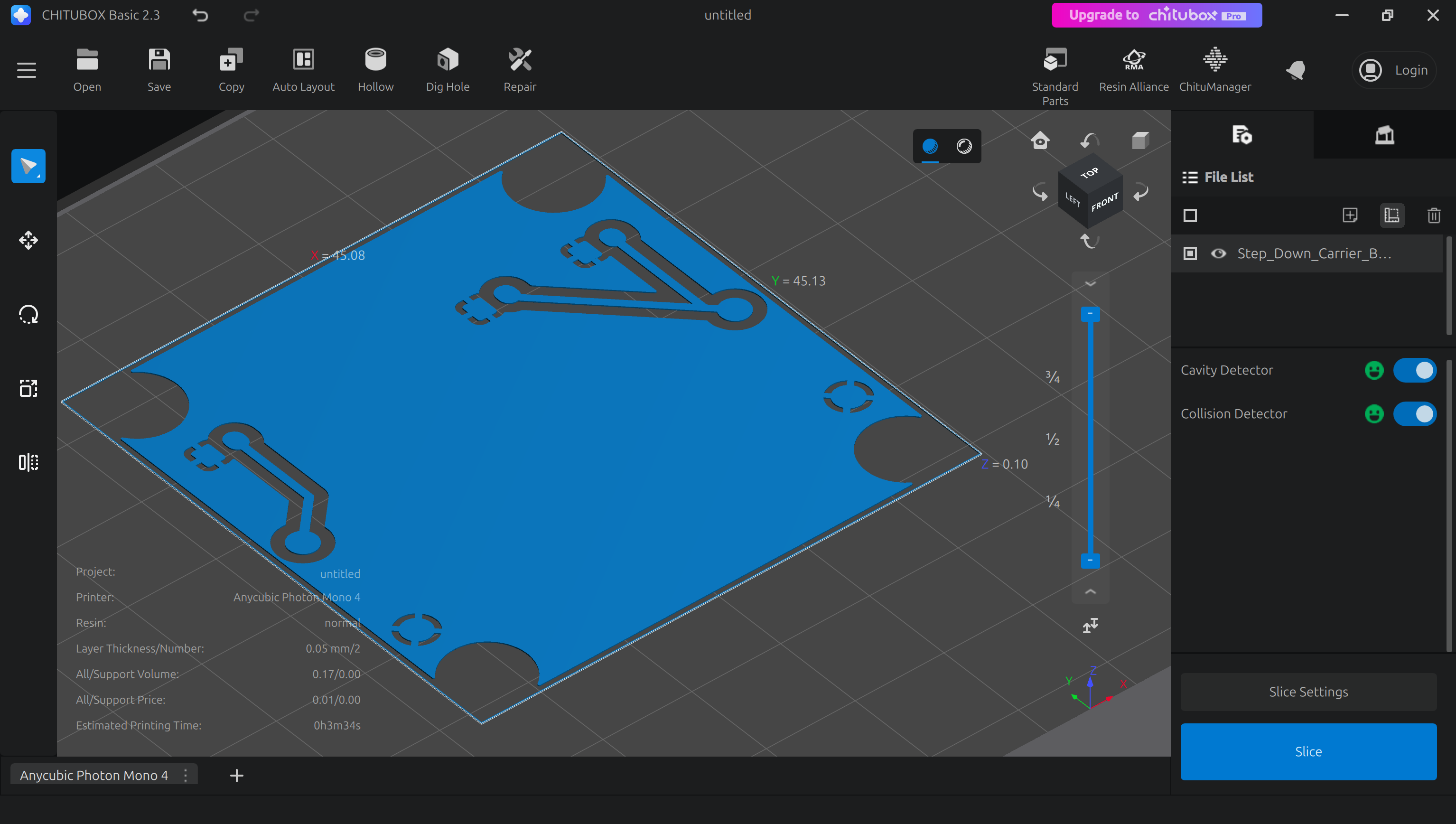
### 3. Slicing in Chitubox
This is where you set the exposure time. The Chitubox slicer (without hacking) requires at least one bottom and one normal layer to be defined. So, the idea is to split the thickness of the model into two or more layers and define the exposure time for each layer.
1. Open Chitubox and import your STL file. Lay it flat on the build plate.
2. Go to the **Parameter Settings**.
#### Exposure Time Examples:
* Pre-sensitized boards from Bungard requre 2 minutes to cure.
* Solder mask in a syringe from Mechanic require 10 minutes to harden.
Since the minimum exposure time per layer is 0.1s and maximum 200s, calculate the total exposure time.
* **1 minutes (60 seconds)**
* Model Thickness (Blender): `0.1 mm`
* Bottom Layer Count: `1`
* Layer Height: `0.05 mm` (creates 2 layer)
* **Bottom Exposure Time:** `60 s`
* **Normal Exposure Time**: `0.1 s` (minimum value)
* **4 minutes (240 seconds)**
* Model Thickness (Blender): `0.1 mm`
* Bottom Layer Count: `1`
* Layer Height: `0.05 mm` (creates 2 layers)
* **Bottom Exposure Time:** `200 s` (max for the first layer)
* **Normal Exposure Time:** `40 s` (for the second layer)
* **10 minutes (600 seconds)**
* Model Thickness (Blender): `0.1 mm`
* Layer Height: `0.025 mm` (creates 4 layers)
* Bottom Layer Count: `1`
* **Bottom Exposure Time:** `0.1 s` (minimum value)
* **Normal Exposure Time:** `200 s` (This will apply to the 3 normal layers, giving 3*200 = 600s total).
4. **Crucially, turn off Anti-aliasing**. Go to the "Advanced" tab and set **Anti-aliasing**. This ensures the sharpest possible pixels for crisp traces.
5. Slice the model and save the file to the USB drive.
### 2. SVG to STL Conversion
The SVG file will be converted to STL in two steps. This can be done manually or with an automated script.
#### Manual Conversion
If you prefer to do all the steps manually, here is the step-by-step guide.
##### Prepare the SVG
**Step 1: Open Your SVG in Inkscape**
Go to **File → Open** and select your SVG.
Remove embedded texts. Embedded texts can be redundant for searchability. To remove them:
1. Press `Ctrl + F` (or go to **Edit → Find/Replace...**).
2. In the panel (usually on the right), under `Options`, look for "Object Type".
3. Uncheck "All Types" (if selected) and check only "Text".
4. Click the **Find** button. All hidden text objects will be selected.
5. Press `Delete` (or go to **Edit → Delete**).
**Step 2: Select Everything**
Press `Ctrl + A` to select all objects on your canvas.
**Step 3: Convert Strokes to Paths**
Go to **Path → Stroke to Path** (`Shift + Alt + C`). This converts any lines into editable paths, which is crucial for Blender.
**Step 4: Unionize Paths**
To combine all separate paths into a single object:
Go to **Path → Union** (`Ctrl ++`).
Your SVG should now appear as a single curve object.
**Step 5: Set Object Dimensions**
In the top toolbar, click on the `lock proportions` icon and set the **width (W:) or height (H:)** of the object.
**Step 6: Export Your Cleaned SVG**
Go to **File → Export**.
Set `DPI` to `1494`, select `Plain SVG` format, set the export path, and click **Export**.
Ensure you export in **Plain SVG** format (not Inkscape SVG) for optimal compatibility with Blender.
##### Convert the SVG to a 3D Model
**Step 1: Open Blender**
Open Blender. In the `Scene Collection`, delete the default cube.
**Step 2: Set Units to Millimeters**
Go to `Scene Properties` (the cone/sphere/cube icon on the right sidebar) and open `Units`.
Set: `Unit Scale: 0.001`, `Length: Millimeters`.
This tells Blender that 1 Blender unit = 1 mm.
**Step 3: Import SVG**
Go to **File → Import → SVG**.
Select the imported object by clicking on its edge.
**Step 4: Convert Object to Mesh**
With the object selected, go to **Object -> Convert -> Mesh**.
**Step 5: Check Dimensions**
Press the `N` key to open the `Transform` panel and look at the `Dimensions`. The Z-axis dimension should be zero.
**Step 6: Add Solidify Modifier**
Click **Add Modifier → Generate → Solidify**.
Set `Thickness: 0.1`, `Even Thickness: yes`, and `Fill Rim: ON`.
Monitor the real thickness displayed on the Z-axis in the `Dimensions` panel.
**Step 7: Export to STL**
Go to **File → Export → Stl (.stl)**.
Check `Apply Modifiers` and save the file.
#### Automated Conversion
This entire workflow can be automated in the Linux terminal using **Inkscape's command-line mode** and **Blender's Python scripting API**.
Use the single shell script [svg2stl.sh](svg2stl.sh) to do the whole job in one go:
**Download:**
```bash
wget https://gitea.virtonline.eu/2HoursProject/svg2stl/raw/branch/main/svg2stl.sh
wget https://gitea.virtonline.eu/2HoursProject/svg2stl/raw/branch/main/pcb_to_stl.py
```
**Setup:**
```bash
chmod +x svg2stl.sh
nano svg2stl.sh
```
Make sure you set the exact width of your model in `TARGET_WIDTH_MM`. Take the width from the outset measurement shown in the KiCad. The height will adjust itself proportionaly. The thickness `THICKNESS_MM` of the model can be adjusted as well. Set the resolution of your 3D printer's screen in `EXPORT_DPI`.
```bash
# Dimensions (Millimeters)
# Set the desired width in mm (e.g. 55.15).
# Leave as "0" to keep the original size from the SVG.
TARGET_WIDTH_MM="45.08"
# Thickness of the 3D model in mm
THICKNESS_MM="0.1"
# Print resolution
# DPI based on the 3D printer resolution (e.g. 1494 for Anycubic Photon Mono 4)
EXPORT_DPI=1494
```
**Usage:**
```bash
./svg2stl.sh my_design.svg
```
### 3. Slicing in Chitubox
This is where you set the exposure time. The Chitubox slicer (without hacking) requires at least one bottom and one normal layer to be defined. So, the idea is to split the thickness of the model into two or more layers and define the exposure time for each layer.
1. Open Chitubox and import your STL file. Lay it flat on the build plate.
2. Go to the **Parameter Settings**.
#### Exposure Time Examples:
* Pre-sensitized boards from Bungard requre 2 minutes to cure.
* Solder mask in a syringe from Mechanic require 10 minutes to harden.
Since the minimum exposure time per layer is 0.1s and maximum 200s, calculate the total exposure time.
* **1 minutes (60 seconds)**
* Model Thickness (Blender): `0.1 mm`
* Bottom Layer Count: `1`
* Layer Height: `0.05 mm` (creates 2 layer)
* **Bottom Exposure Time:** `60 s`
* **Normal Exposure Time**: `0.1 s` (minimum value)
* **4 minutes (240 seconds)**
* Model Thickness (Blender): `0.1 mm`
* Bottom Layer Count: `1`
* Layer Height: `0.05 mm` (creates 2 layers)
* **Bottom Exposure Time:** `200 s` (max for the first layer)
* **Normal Exposure Time:** `40 s` (for the second layer)
* **10 minutes (600 seconds)**
* Model Thickness (Blender): `0.1 mm`
* Layer Height: `0.025 mm` (creates 4 layers)
* Bottom Layer Count: `1`
* **Bottom Exposure Time:** `0.1 s` (minimum value)
* **Normal Exposure Time:** `200 s` (This will apply to the 3 normal layers, giving 3*200 = 600s total).
4. **Crucially, turn off Anti-aliasing**. Go to the "Advanced" tab and set **Anti-aliasing**. This ensures the sharpest possible pixels for crisp traces.
5. Slice the model and save the file to the USB drive.
 ### 4. Exposing the Board
1. **IMPORTANT:** Remove the resin vat and the build plate from your printer. You only need the LCD screen and the UV light source. Protect the screen with a spare FEP film or a screen protector.
2. Place your pre-sensitized PCB directly on the protected LCD screen.
3. Put same weights on the PCB to keep it flat. You also can create a jig that would keep the double-sided board aligned.
4. Insert the USB drive containing the 3D model.
5. Start the "print". The printer will expose the board using the layer images and times you configured.
### 5. Developing
1. After exposure, you must develop the board to reveal the pattern.
* For a **positive photoresist board** (like the Bungard brand), the developer is a weak alkaline solution. A common and effective developer is a **1% solution of Sodium Hydroxide (NaOH)** in distilled or demineralised water.
* For a **negative dry film resist**, the developer is a solution of Sodium Carbonate (washing soda). Mix approximately 10 grams of sodium carbonate per liter of warm water until dissolved.
* For the UV light curing solder mask, allow more time to it to harden. Clean the uncured part with Izopropanol afterwards.
2. **Safety First:** When working with chemicals like NaOH or Sodium Carbonate, always wear gloves and eye protection.
3. Submerge the board in the appropriate developer solution and gently agitate it. This should take 30-90 seconds, depending on the resist and developer freshness.
4. Rinse the board thoroughly with water.
### 4. Exposing the Board
1. **IMPORTANT:** Remove the resin vat and the build plate from your printer. You only need the LCD screen and the UV light source. Protect the screen with a spare FEP film or a screen protector.
2. Place your pre-sensitized PCB directly on the protected LCD screen.
3. Put same weights on the PCB to keep it flat. You also can create a jig that would keep the double-sided board aligned.
4. Insert the USB drive containing the 3D model.
5. Start the "print". The printer will expose the board using the layer images and times you configured.
### 5. Developing
1. After exposure, you must develop the board to reveal the pattern.
* For a **positive photoresist board** (like the Bungard brand), the developer is a weak alkaline solution. A common and effective developer is a **1% solution of Sodium Hydroxide (NaOH)** in distilled or demineralised water.
* For a **negative dry film resist**, the developer is a solution of Sodium Carbonate (washing soda). Mix approximately 10 grams of sodium carbonate per liter of warm water until dissolved.
* For the UV light curing solder mask, allow more time to it to harden. Clean the uncured part with Izopropanol afterwards.
2. **Safety First:** When working with chemicals like NaOH or Sodium Carbonate, always wear gloves and eye protection.
3. Submerge the board in the appropriate developer solution and gently agitate it. This should take 30-90 seconds, depending on the resist and developer freshness.
4. Rinse the board thoroughly with water.